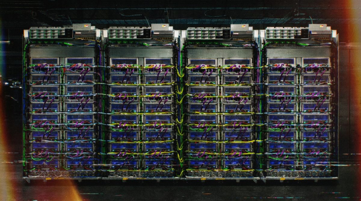
Google has introduced the TPU 8tx and the TPU 8i Max, expanding its eighth-generation AI accelerator lineup to challenge the cost profile of enterprise model serving. Across the industry, the commercial focus is shifting from expensive model training runs toward day-to-day inference, turning hardware procurement into an ongoing operational expense. For the first time, Google has shipped four TPU systems within a single year, altering its hardware expansion tactics by relying entirely on existing silicon rather than deploying a new processor generation.
This architecture bypasses typical silicon fabrication cycles by altering packaging, inter-chip networking, and memory allocations around the existing core processor. Operating teams avoid multi-year tape-outs by taking a modular engineering approach that, according to Google, lets it deliver operational hardware variants in months rather than years. Instead of selling a single general-purpose compute block for every server rack, the infrastructure provider delivers targeted rack-level systems to capture external inference workloads away from Nvidia. By optimizing procurement economics around existing silicon, corporate data centers can scale inference capacity without waiting for new fabrication nodes.
Targeted Silicon Against Monolithic Architectures
Each variant targets specific architectural boundaries that inflate corporate data center overhead. The TPU 8tx addresses enterprise data security by isolating model weights and active workloads so information remains encrypted throughout live calculations. For regulated sectors, this architectural change prevents data exposure without forcing corporate teams to move information across isolated clusters.
The TPU 8tx keeps confidential data encrypted during processing while the TPU 8i Max doubles memory and compute power in the same rack format.
This continuous encryption setup operates on the low-latency Boardfly network Google built for live inference tasks, designed to yield up to twice the latency reduction compared to the earlier TPU 8t, thereby mitigating the real-time response bottlenecks common in large-scale model deployments. Meanwhile, long-context models and enterprise agents face severe data-transfer bottlenecks when processing extensive codebases or video streams. Google countered this chokepoint by combining two TPU 8i chips directly onto a single physical package inside the TPU 8i Max. The resulting system yields double the compute capacity, double the memory, and double the memory bandwidth within identical rack dimensions, doubling processing output per square meter of facility footprint.
Software Layers and Ecosystem Friction
The central hurdle to enterprise migration remains whether custom modular hardware assemblies can displace Nvidia's established data center architecture. Nvidia already fields an active confidential computing architecture on its own GPUs, defending its dominant footprint through deeply rooted software ecosystems. To counter this friction, Google released TorchTPU as an open-source tool designed to execute standard PyTorch code on TPUs with minimal structural edits, while integrating native support for inference frameworks including vLLM and SGLang.
Specialized chips like TPUs can play to their strengths in day-to-day inference as tech giants race to deploy in-house accelerators.
This hardware expansion reflects an operational push across hyperscale operators looking to curtail accelerator expenditures, with Amazon, Microsoft, and OpenAI similarly designing in-house chips. Nvidia has moved to fortify its own inference portfolio via an acqui-hire and licensing agreement with Groq, defending its pricing power as infrastructure buyers weigh specialized rack configurations. Google currently counts nearly 100 external TPU customers running on its platform.
What doesn’t add up
Google rolled out a record four chip configurations in a single year, yet it did not fabricate a single new processing core for them. Rather than waiting through multi-year tape-out cycles, the company simply repackaged existing silicon with modified interconnects and memory, slashing turnaround times while leaving the core software barrier intact. Open tooling like TorchTPU and direct hooks into vLLM barely scratch the surface of unseating Nvidia’s deeply entrenched data-center dominance. Will modular packaging and halved network latency be enough to lure enterprise inference workloads away from Nvidia's confidential-computing clusters?