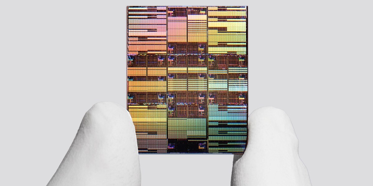
The semiconductor industry has hit a wall: the race to shrink a transistor’s horizontal footprint has shifted from an engineering challenge into a desperate war against the laws of physics. While Moore's Law relied on miniaturization for decades, the sub-10-nanometer scale introduced quantum mechanics, which began dictating its own rules for switching functions. IBM’s answer is not further compression, but verticality. The company’s new chip prototype signals a radical pivot: instead of crowding a flat surface, transistors are growing upward. On a surface the size of a fingernail, IBM has managed to pack 100 billion transistors, doubling the density of its own 2021 records.
Nanostack Architecture
The technology IBM calls "nanostack" is a departure from the flat-plan development that has dominated the market for decades. Unlike traditional solutions where transistors sit side-by-side, the nanostack utilizes a Complementary Field-Effect Transistor (CFET) design. Here, devices are layered like a sponge cake: engineers form the first layer on the silicon, cover it with a second layer of material, and build the next batch of transistors directly on top.
CFET-based (Complementary FET) architecture allows p-type and n-type transistors to be stacked vertically. Logic element density doubles within the same crystal footprint. Projected performance gains for operations reach 50%.
"This approach will become universal for both GPUs and CPUs," notes Huiming Bu, IBM’s VP of Semiconductor R&D.
Dan Hutcheson of TechInsights suggests that vertical stacking extends the industry roadmap by another 10–15 years, enabling significantly more computation within the same physical dimensions.
Solving the Data Center Energy Crisis
The economics of this vertical shift are tied to the catastrophic surge in AI infrastructure power consumption. Modern data centers have effectively hit a thermal and electrical ceiling. Jay Gambetta, Director of IBM Research, states bluntly that nanostack chips will become mainstream within the decade specifically to prevent facilities from being incinerated by their own electricity bills.
According to IBM’s internal estimates, these 3D chips could be up to 70% more energy-efficient than their predecessors. In a world where power shortages are throttling the training of next-generation LLMs, efficiency becomes more critical than raw performance.
IBM's move to vertical nanostacking is a tactical admission that traditional silicon scaling is exhausted. Doubling transistor density and promising a 70% efficiency boost gives Moore's Law a ten-year reprieve. For business leaders, this represents a paradigm shift: the primary lever for managing Total Cost of Ownership (TCO) in data centers is no longer purchasing terawatts of power, but the architectural density of the systems themselves. The era of hardware "brute force" is ending, making way for vertical arbitrage.