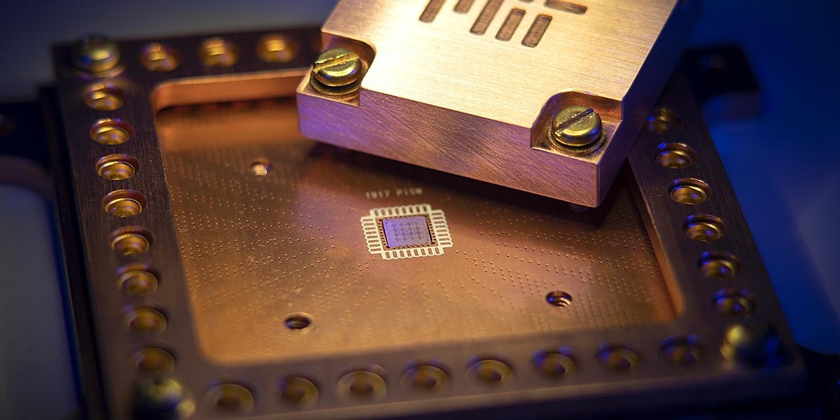
Quantum computing remains one of the most formidable frontiers in technology, facing a myriad of engineering bottlenecks. Chief among these are two critical hurdles: miniaturization and qubit quality. According to current industry roadmaps, such as IBM’s, the standard goal was to achieve a 1,121-qubit processor by 2023. However, contemporary methods necessitate either massive chips—measuring over 50 millimeters per side—or complex multi-chip modules. The reliance on coplanar capacitors in current circuitry is driven by the need to dissipate electric fields and compensate for defects in materials like silicon oxide or silicon nitride, which are simply too imperfect for the rigorous demands of quantum systems.
Researchers at the Massachusetts Institute of Technology (MIT) have unveiled a solution to these persistent challenges. A team led by William Oliver, director of the MIT Center for Quantum Engineering, utilized two-dimensional materials, specifically the insulator hexagonal boron nitride (hBN). This innovation has enabled a 100-fold increase in the number of superconducting qubits that can be integrated onto a single device. The researchers demonstrated that several atomic monolayers of hBN can be stacked to form the dielectric layer within the capacitors of a superconducting qubit. As Oliver points out, merely scaling the number of qubits is insufficient for quantum computing; they must also maintain high performance. Sacrificing quality for quantity is a dead end; both metrics must advance in tandem.
This new architecture addresses the low quality of standard insulators, which exhibit excessive defects at temperatures below 0.02 Kelvin (just above absolute zero). Integrating hBN into superconducting circuit capacitors not only saves space but also reduces crosstalk between neighboring qubits. MIT researchers emphasize that this synergy of miniaturization and stability is the key to scalability, allowing high-performance computing elements to be packed significantly more densely than ever before.