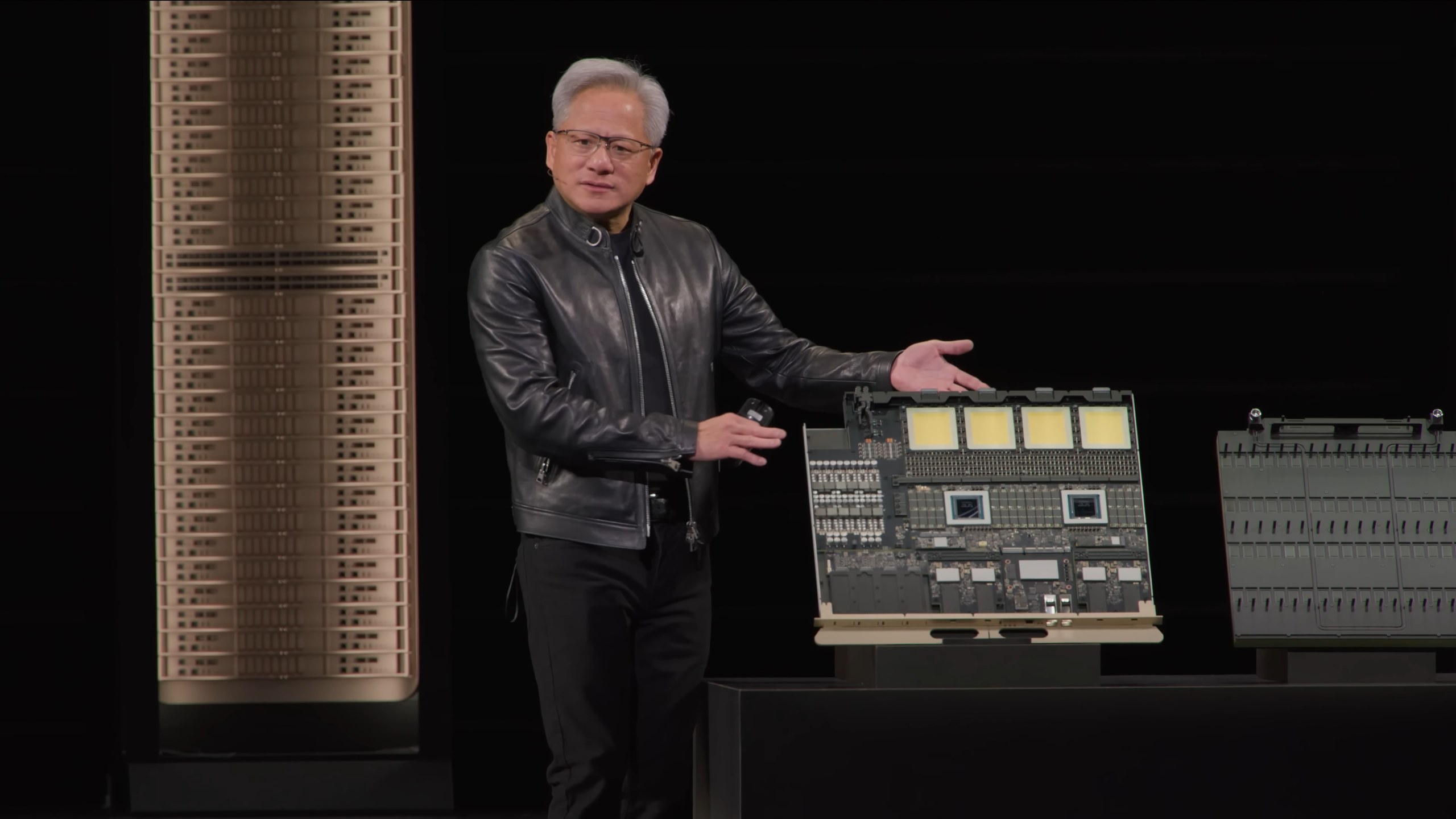
Nvidia’s roadmap is hitting a physical wall as the global shortage of High Bandwidth Memory (HBM) forces a tactical retreat from Jensen Huang’s flashy stage promises. According to reports from The Information and deep dives by SemiAnalysis, the green giant is currently testing versions of its upcoming Rubin Ultra accelerator with memory capacities that look more like a downgrade than a revolution. While the GTC marketing slides teased a design boasting 1 TB of HBM4E memory, the reality of a choked supply chain has forced prototypes down to a meager 192 GB or 256 GB. This isn't just a slight trim; it’s a wholesale departure from the Kyber NVL144 vision that was supposed to redefine large-scale model training.
Technical Downgrades and the Memory Wall
The pivot from HBM4E to standard HBM4 in these test configurations is a glaring symptom of manufacturing exhaustion. HBM4E was marketed as the holy grail—offering a customizable base logic die through partnerships between Micron and TSMC. However, complexity has its price, and that price is a production bottleneck. As noted by Tom’s Hardware, memory manufacturers simply cannot keep pace with the specs required for the Rubin Ultra rollout. Furthermore, analysis suggests Nvidia has scrapped the ambitious quad-die design for Rubin Ultra, opting instead for a more conservative dual-GPU setup. While a dual-die configuration makes lower memory capacities technically logical, the 192 GB specs under testing are actually lower than the 288 GB found in current base Rubin GPUs. It’s a retreat disguised as a roadmap.
For CTOs and infrastructure planners, the narrative has shifted. The bottleneck is no longer the raw power of the transistor, but the availability of the memory that feeds it. This supply lock-in means that despite Nvidia’s cozy relationship with SK hynix, physical production limits are now dictating the performance ceilings of next-generation hardware. The forced transition to standard HBM4 will inevitably throttle the bandwidth available for training the next frontier of LLMs, shifting the burden of performance from single-chip brilliance to the expensive, complex world of cluster-level scaling.
The Shift to Software Optimization and Infrastructure TCO
The economic fallout is equally sobering. With the NVL144 rack originally slated for 2027 now likely pushed to 2028, the timeline for AI ROI is stretching. While Nvidia insists its "roadmap is intact," the company has been notably silent on whether these specific delays are real. A one-year slip combined with lower per-GPU memory fundamentally breaks the Total Cost of Ownership (TCO) models for Big Tech. To hit the computational benchmarks promised for 2027, enterprise buyers will be forced to buy more racks to compensate for the memory deficit. The era of "brute force" hardware gains is hitting a plateau, placing a desperate premium on software optimization to squeeze blood from increasingly stagnant silicon.
This landscape suggests a period of architectural stagnation where the gap between marketing demos and shippable hardware is becoming a canyon. The reliance on a tiny cabal of suppliers—SK hynix, Samsung, and Micron—is now the undisputed Achilles' heel of the AI transformation. For those holding the checkbook, the strategy must pivot: stop waiting for the next annual hardware miracle and start focusing on architectural efficiency. Nvidia’s engineering teams are quietly testing 192 GB prototypes to see if the market will blink at a 2028 release that looks suspiciously like today’s tech. The roadmap may be "intact" on paper, but the disappearing memory and shifting dates tell a far more grounded story.