Merging Synthetic DNA and Perovskite Semiconductors
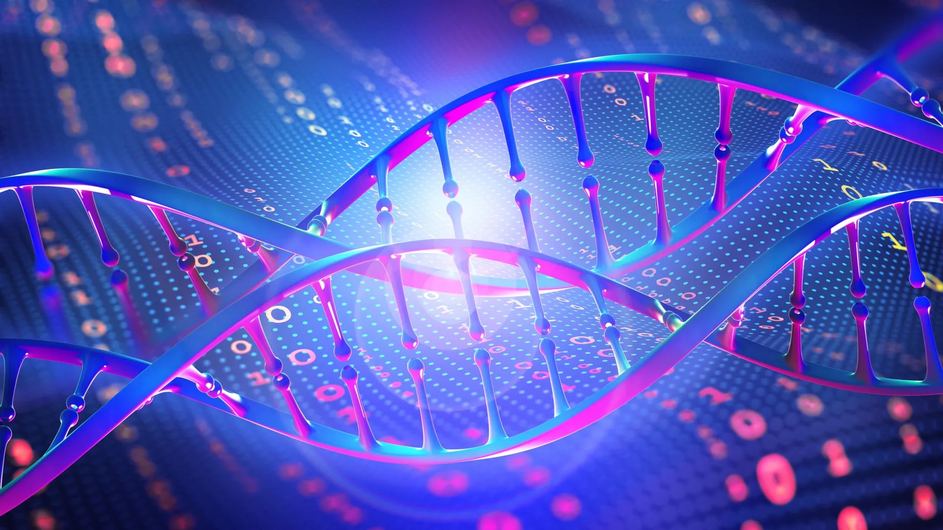
Penn State researchers have built a bio-hybrid memristor that couples synthetic DNA directly with a semiconductor substrate, executing in-memory computing at power levels two orders of magnitude below conventional solid-state hardware. As detailed in Advanced Functional Materials and an accompanying patent filing, the architecture tackles the von Neumann bottleneck by collapsing chemical data storage and active processing into a single physical site.
While natural DNA boasts an theoretical storage density of 215 petabytes (roughly 215 million gigabytes) per gram, harnessing biological strands in electronic circuits has historically stalled on structural degradation and low conductivity. As Kavya S. Keremane, co-corresponding author and postdoctoral researcher in materials science and engineering at Penn State, explained, bridging biology and electronics required developing a novel materials platform so the two domains could operate seamlessly together. The team bypassed messy biological extractions by pairing short, rigid synthetic DNA sequences with crystalline perovskite—a semiconductor already proven in optoelectronics and solar cells.
Low-Power In-Memory Architecture
Instead of wrestling with the entanglement and fragility of natural polymers, the engineered short oligonucleotides provide a stable matrix that modulates ionic transport. The resulting memristor retains a record of historical electrical activity by tracking prior current flow even when power drops entirely.
This non-volatile state retention enables true in-memory processing, mirroring biological synapses that compute and store state concurrently. For AI infrastructure facing a thermal wall and unsustainable energy footprints as model parameter counts explode, bypassing constant data shuttling between discrete memory and logic units is an engineering imperative rather than a luxury.
What this means
The Penn State demonstration offers a rigorous proof-of-concept for biomolecular memristive switching, but the engineering roadmap to commercial silicon replacement remains steep. Transitioning from an academic patent to enterprise-grade accelerators demands solving severe read/write latency bottlenecks, proving molecular stability under continuous thermal cycles, and engineering bio-compatible packaging that won't poison standard foundry cleanrooms.