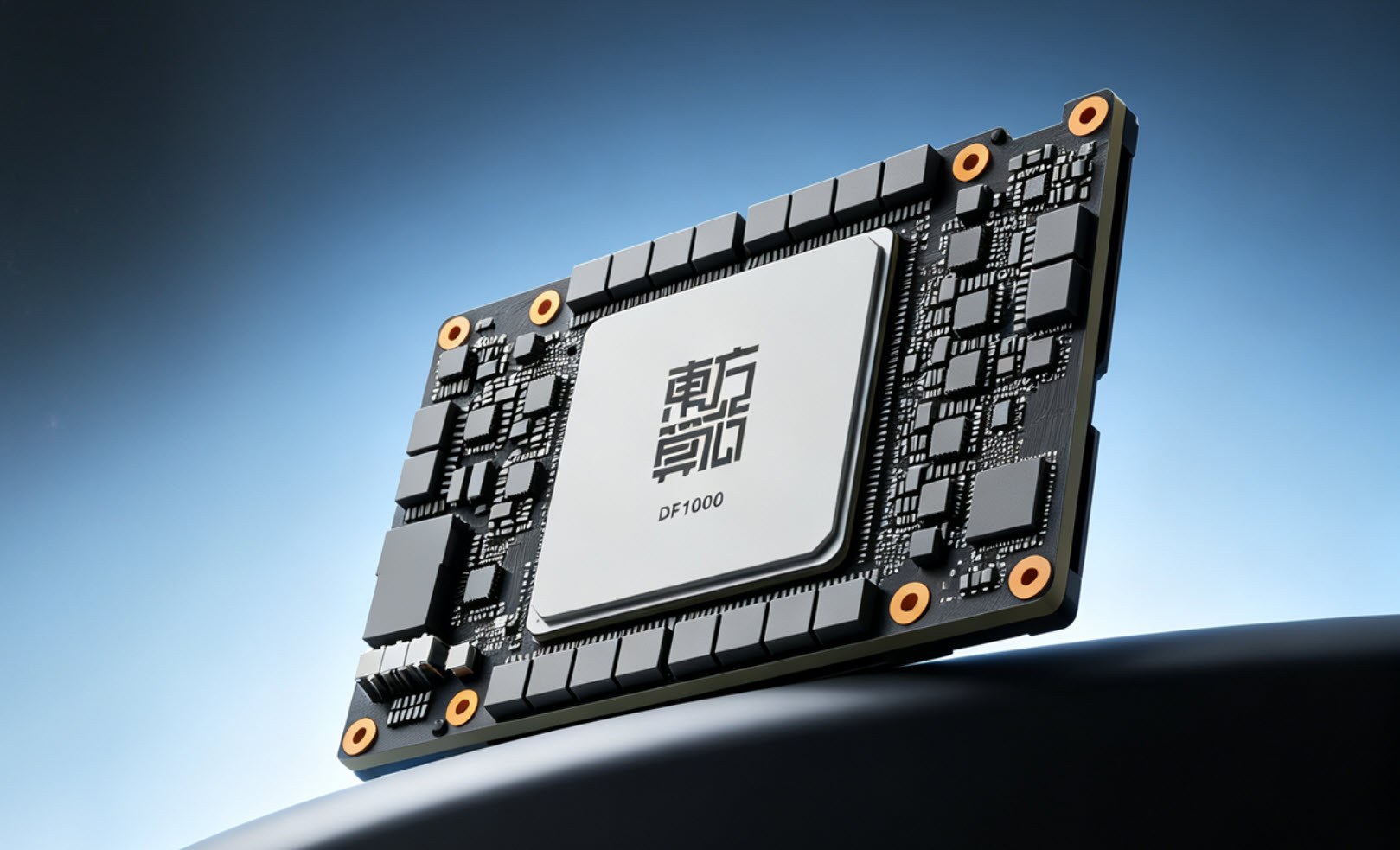
The global race for AI supremacy has long resembled a fetishization of nanometers, but Chinese firm Dongfang Suanxin (DFSX) is moving the battlefield to memory architecture. While Western giants scramble for access to EUV lithography, DFSX is highlighting the obvious: the primary bottleneck in AI today isn't a lack of raw teraflops, but the so-called "memory wall." GPUs sit idle waiting for data, and no amount of transistor miniaturization can solve this within a classic layout.
Instead of chasing 5nm nodes, DFSX is utilizing mature 14nm capacity to build its DF1000 and DF2000 chips, betting entirely on bandwidth. This isn't merely a survival tactic under sanctions; it's a pragmatic shift from a compute-centric to a memory-centric paradigm. The technical core of this strategy is wafer-level hybrid bonding. As DFSX explains, this method allows copper interconnects between memory and logic layers to be joined directly, bypassing micro-bumps or traditional wire bonding. The resulting architecture resembles a system of millions of high-speed vertical elevators rather than a horizontal highway plagued by traffic jams, radically slashing latency.
DFSX posits: it is the "memory wall," not the process node, that truly limits performance today.
Strategic context
Set for a late 2026 release, the DF2000 chip is evolving into a "3.5D Infinity Chiplet" structure. This design places multiple memory towers and compute units on a single substrate, replacing standard modules with custom 3D DRAM integrated right into the silicon. By bringing data this close to logic, the DF2000 hits a staggering 15 TB/s per chip. Granted, the TY64 SuperNode’s raw BF16 compute performance sits at 64 PFLOPS—paling in comparison to the 360 PFLOPS of NVIDIA’s GB200 NVL72. However, DFSX is banking on the fact that in real-world LLM training, the speed at which you "feed" the processors matters more than their theoretical peak power.
The economics of scaling under equipment shortages support this asymmetric response. A TY64 SuperNode configured with DF2000 chips delivers a massive 960 TB/s of memory bandwidth. For context, NVIDIA’s flagship GB200 NVL72 offers only 576 TB/s. Even accounting for NVIDIA’s upcoming Vera Rubin system, expected to hit 1,580 TB/s, the projected Chinese DF3000 chip will push the TY64 to 1,280 TB/s. The bottom line: NVIDIA’s top-tier solution may retain only a 23% lead in bandwidth despite using lithography that is several times more expensive and complex.